Can your board designs save money?
Can Your Board Designs Save Money?
In contract manufacturing we come across many board designs which vary from the simplest 2-layer board to complex technology in a 26-layer HDI impedance-controlled flexi-rigid design.
The question is how manufacturable are your designs? Secondly, have you thought about the cost of manufacturing and by this we don’t mean the cost of components and materials, but the cost of manufacturing to your PCBA designs.

As part of our ongoing improvement ethos, we look at how to save you cost by implementing good pad designs at the layout stage and reducing the potential for component placement issues, costly rework, or in the worst scenario, potentially scrapped boards.
With 0201 package sizes being commonplace now, at NOTE Windsor we conducted some 0201 component placement trials to identify how to improve yields on a specific project.
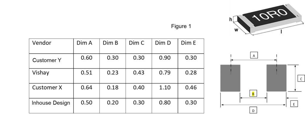
Using four different pad designs; two from customers, one from Vishay and an alternative inhouse design, we produced a sample panel that was identical on both sides to offer 8 trial circuits with varying dimensions as shown in Figure 1.
The stencil was produced with varying aperture designs for each circuit as illustrated in Figure 2.
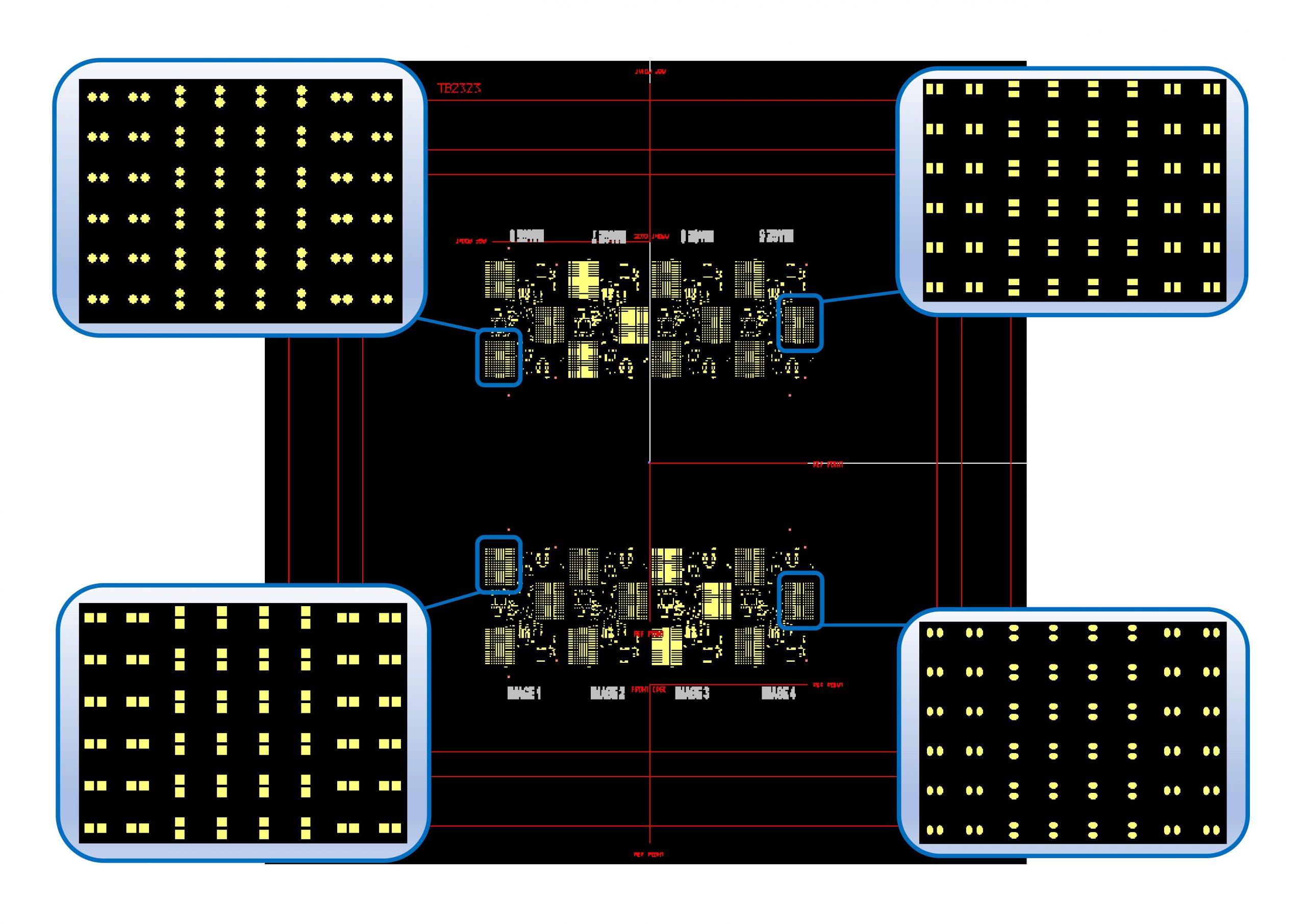
Side 1
Image 1 = Square & Rectangle 1 to 1
Image 2 = Round & Obround 1 to 1
Image 3 = Square & Rectangle -10% from inside edge
Image 4 = Round & Obround 1 to 1 -10% from inside edge
Side 2
Image 5 = Square & Rectangle 10% Increase in width
Image 6 = Round & Obround 10% Increase in width
Image 7 = Square & Rectangle -10% from back edge
Image 8 = Round & Obround -10% from back edge
Trial Results
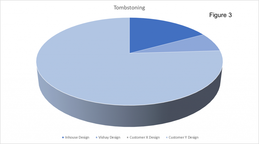
Using fresh OM340 paste from Alpha and a selection of capacitors and resistors, an equal number of each was placed and the trial yielded the following results in terms of tombstoned components.
Inhouse Pad Design 17%
Vishay Pad Design 7%
Customer X Pad Design 0%
Customer Y Pad Design 76%
Conclusions drawn from this trial clearly indicate that the dimension ‘B’ in Figure 1 is critical and ideally when we are designing boards, we should aim for a pad gap of 0.2 or slightly less. This gap is often a global setting within CAD layout software but can be adjusted so your library of component layouts uses your preferred pad gap. Interesting is the marked difference between the project we were looking to improve yield on with Customer Y and the results yielded by Customer X’s design which produced the best results.
Pad Size
Another aspect of design that contributes to tombstoning, is having one pad larger than the other. This will also potentially result in the components being pulled and twisting during reflow. The examples in Figure 4, of components with different pad sizes, should ideally be avoided.

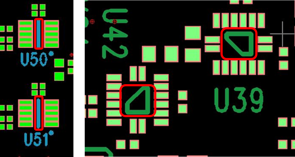
Thermal Relief
Provisioning for Thermal Relief is the third factor we consider, simple guidelines for which are shown in Figure 5. Again, this is often a global setting within CAD software, but equally can be done by hand on those intricate designs where the software algorithms are less successful. If not included the results can be uneven thermal reflow and components pulled off centre or tombstoned as one pad reflows faster than the other.
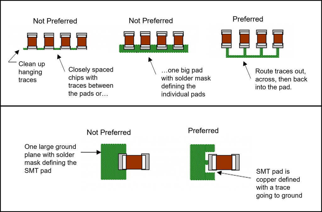
Figure 6 shows examples of uneven thermal relief which has the potential for causing tombstones and uneven reflow.
Silkscreen
Our third point to consider is whether Silkscreen underneath components such as DFNs, QFNs & leadless devices is required. In some instances, this can result in them not sitting flat on the board, causing components to lift on one side and not reflow correctly. The layout examples in Figure 7 highlight examples of silkscreen underneath components which could be removed. In a separate trial our customer removed the silkscreen from their design, and we noticed a marked improvement in repeatability of placement.
Component Proximity
Designing your mixed technology boards has never been more critical with processes like automated selective solder on offer from most manufacturers. At NOTE we have multiple Selective Solder systems with two lines located in Windsor UK. Figure 8 shows examples of the kind of issues one should aim to avoid where small SMD components are located next to through hole components.
If one wants to benefit from this type of process, then SMD components in close proximity to the board edge or through hole components make selective soldering challenging or sometimes impossible.
Ideally one requires them to be placed 3mm apart which is often huge in terms of real estate on small boards, but this process does depend on access to pins with selective soldering. Do take a look at our video channel on YouTube featuring this process technology.
Top Tips To Consider
- Component Pad Design
- Component Pad Gaps
- Pad Size
- Thermal Relief
- Silkscreen
- Component Proximity
EXPERIENCE THE DIFFERENCE
See why NOTE is right for you.
Contact us today to discuss your needs.